Categories
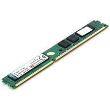
Kingston ValueRam 8GB (1x 8GB) DDR3 1600MHz Memory
AU$62.73
In stock
1
Kingston ValueRam 8GB (1x 8GB) DDR3 1600MHz Memory
Product Details
Brand: Kingston
Kingston ValueRam 8GB Desktop Memory - DDR3 1600MHz - 240Pin Dimm - CL11 - Non-ECC - SR x8 (KVR16N11/8)
- Manufacturer Warranty: 12 Months Limited Warranty
- Manufacturer Contact Info: http://www.kingston.com/en/, 1800 620 569
FEATURES
- JEDEC standard 1.5V (1.425V ~1.575V) Power Supply
- VDDQ = 1.5V (1.425V ~ 1.575V)
- 800MHz fCK for 1600Mb/sec/pin
- 8 independent internal bank
- Programmable CAS Latency: 11, 10, 9, 8, 7, 6
- Programmable Additive Latency: 0, CL - 2, or CL - 1 clock
- 8-bit pre-fetch
- Burst Length: 8 (Interleave without any limit, sequential with starting address ì000î only), 4 with tCCD = 4 which does not allow seamless read or write [either on the fly using A12 or MRS]
- Bi-directional Differential Data Strobe
- Internal(self) calibration : Internal self calibration through ZQ pin (RZQ : 240 ohm ± 1%)
- On Die Termination using ODT pin
- Asynchronous Reset
- PCB : Height 1.180î (30.00mm), double sided component
Display prices in:AUD
